
How EUV technology can break through to support the explosive growth of the AI revolution
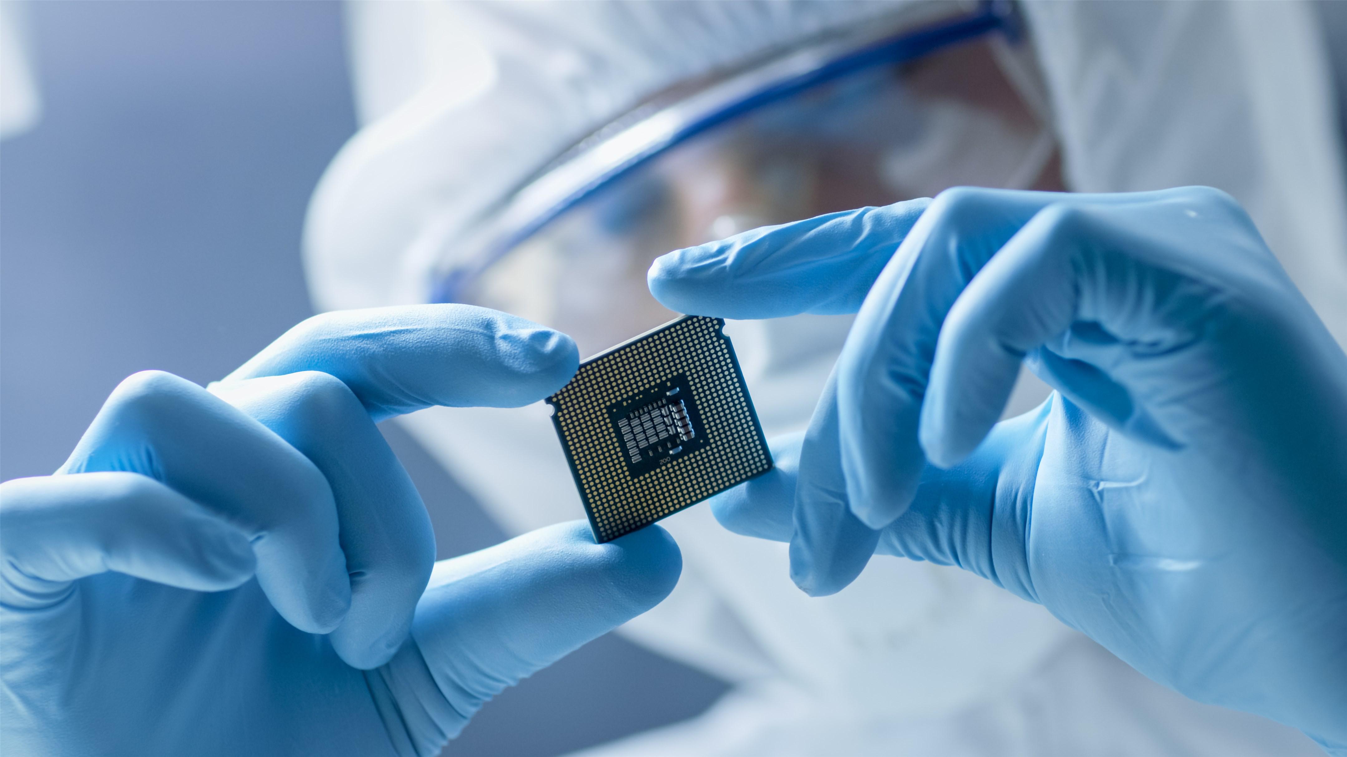
The demand for advanced process chips that support the artificial intelligence revolution has exploded, and it is continuously testing the supply capacity of the global semiconductor industry. From hyperscale data centers that support large language models to edge AI in smartphones, IoT devices, and autonomous driving systems, the thirst for cutting-edge semiconductors in various fields has formed a superimposed effect. However, the manufacturing of such chips is highly dependent on extreme ultraviolet (EUV) lithography technology, and the scale bottleneck of the technology itself has become a key obstacle to the development of the industry.
Since the first batch of commercial EUV chips came out in 2019, continuous improvements in equipment iteration, mask generation, and photoresist technology have stabilized the technology. Although the yield continues to improve, there is still a significant gap compared with the more mature deep ultraviolet (DUV) lithography. Process stability requires continuous monitoring and fine-tuning, and the high investment in power generation equipment, special equipment, and consumables makes the popularization of EUV technology still face economic challenges.
AI demand curve verticalization
The demand for AI computing power is showing a vertical growth trend, directly reshaping the semiconductor industry landscape. AI workloads, high-bandwidth memory (HBM) and new-generation mobile computing devices are jointly driving the evolution of process nodes towards a more refined direction. Each technological iteration means a more complex EUV manufacturing process, among which high numerical aperture (High-NA) EUV has become the only feasible solution for mass production of 1.8 nanometers and below.

Nvidia, AMD and Intel's cutting-edge AI chips have generally adopted 5nm and 3nm processes manufactured by EUV, and the evolution to 2nm all-around gate (GAA) transistors will further increase the dependence on EUV technology.
In the field of HBM, Samsung, Micron and SK Hynix are selectively deploying EUV technology. Although the storage cell array is still mainly based on DUV, key parts such as logic circuits have begun to introduce EUV technology to improve density and precision.
In addition to AI and HBM, the next-generation logic devices used for 5G, autonomous driving systems and edge computing will also require the resolution advantages of extreme ultraviolet lithography (EUV) technology on certain key layers. The fundamental challenge is that, despite the exponential growth in demand for AI chips, the number of fabs capable of producing EUV-based chips remains limited.
Currently, only five companies in the world, TSMC, Samsung, Intel, SK Hynix and Micron, have the ability to mass-produce EUV, and together they control the global supply of 5nm process. Japan's Rapidus Alliance joins the battle with the Hokkaido IIM-1 fab, planning to achieve EUV mass production in 2027, but the industry oligopoly is unlikely to change in the short term.
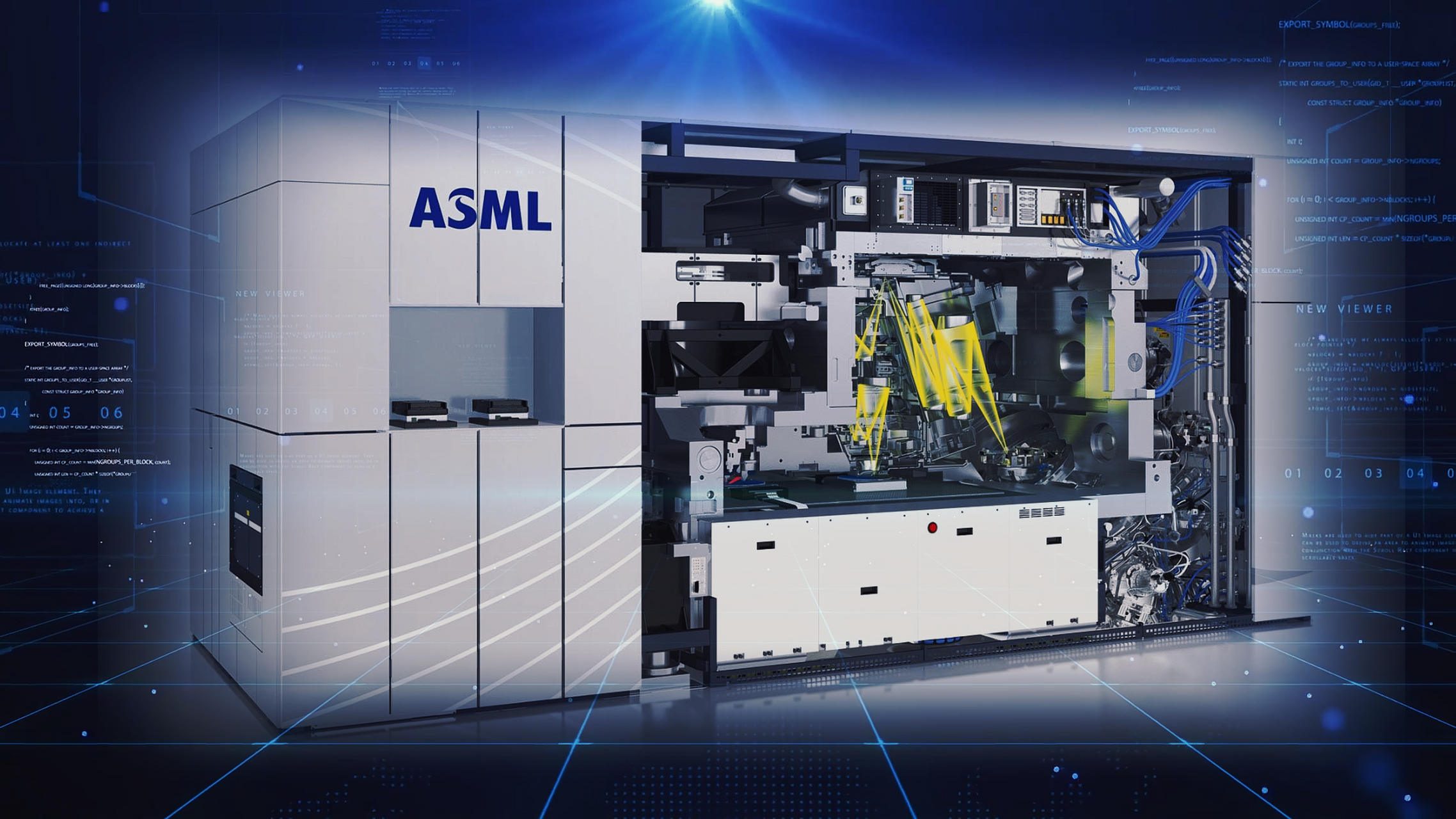
ASML, as the only supplier of EUV equipment, has a backlog of orders for more than three years. TSMC's US plant, Intel's European and American expansion projects, and Samsung's Texas foundry plans are thirsting for EUV equipment, causing the supply-demand gap to continue to widen. It is predicted that the AI chip market will expand to 10 times its current size in the next 5-7 years, and TSMC's 2nm process order schedule has been extended to 2026.
EUV equipment bottleneck
Faced with the EUV equipment bottleneck, government-supported research centers have actively intervened. Facilities such as imec in Belgium and the EUV Accelerator, funded by the US CHIPS Act, are focused on advancing EUV mask technology, process control, and resist chemistry to improve yield and reduce cost per wafer.
imec plays a key role in testing and validating next-generation mask materials that improve feature resolution while reducing random defects. EUV Accelerator accelerates manufacturing and industry adoption by providing cutting-edge EUV tools and research platforms
Due to EUV usage and cost constraints, many leading fabs are turning to innovative lithography strategies. Hybrid lithography has become the standard, where EUV is used only for the most critical layers, while 193nm ArF, ArF immersion, and KrF (248nm) scanners handle less demanding features. Multiple patterning techniques, such as double and quadruple patterning, have also significantly expanded the application range of DUV, allowing fabs to produce smaller feature sizes without EUV investments. In addition, some companies are exploring technologies such as nanoimprint lithography (NIL) and self-assembly patterning of specific layers.
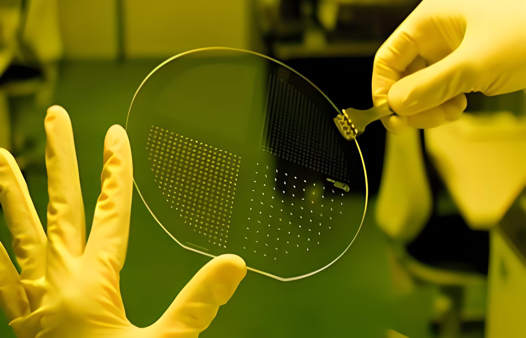
EUV lithography also faces challenges with mask infrastructure. The reflective structure of EUV masks introduces new failure modes, where tiny defects can cause patterning failures, increase defectivity, and reduce yield.
To address this issue, researchers are working on improving multi-beam mask writers, high-transparency pellicles, and achieving defect-free mask blanks. Multi-beam electron beam mask writing technology significantly reduces the time required to create high-precision, defect-free masks. Traditional single-beam mask writers are slow and prone to pattern errors, but multi-beam systems use thousands of parallel electron beams to speed production while maintaining sub-nanometer accuracy.
Thin film technology, which is the protective layer on the mask, has also made significant progress. Early EUV pellicles were very fragile and had low transmission efficiency, which reduced scanner productivity. New carbon-based pellicles have significantly improved thermal stability and transmission, extending the life of the mask without degradation. This in turn reduces the need for frequent mask replacement, which is an expensive and time-consuming process. It also improves consistency between wafers.
Advances in mask durability, pattern fidelity, and overall defect control are helping fabs push EUV yields to levels comparable to more mature DUV technologies, but mask costs remain a significant financial burden. The industry is actively working to address these economic and technical challenges.
Material progress
Photoresist materials are also a key challenge in achieving high yield and process stability for EUV lithography. Although chemically amplified photoresist (CAR) has long been the industry standard, it faces problems such as acid diffusion and random defects at advanced nodes, limiting its ability to meet the requirements of next-generation semiconductor manufacturing.
To overcome these limitations, the industry is actively exploring alternative technologies such as metal oxide photoresist (MOR), Aether dry photoresist technology, and multi-trigger photoresist (MTR). MOR has strong absorption and good contrast at EUV wavelengths, but is sensitive to process conditions; Aether dry photoresist technology applies MOR through vapor deposition, which enhances process control; MTR uses small molecules to achieve smaller feature sizes and higher resolution, and uses a controlled catalytic process to reduce acid diffusion. However, these photoresist platforms all have their own process sensitivities that need to be addressed by wafer fabs.
As semiconductor manufacturers transition to high-NA EUV, these material limitations will become more pronounced, requiring new photoresists and substrates that break the boundaries of molecular engineering. While no single photoresist platform currently meets all EUV requirements, ongoing advances in CAR, MOR, MTR, and dry photoresists represent multiple pathways to addressing EUV’s most pressing material challenges.
AI Process Control
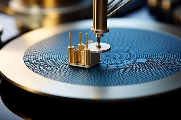
Fabs are increasingly relying on AI and machine learning technologies for process control. AI-driven metrology tools developed by companies such as Tignis and Synopsys can analyze process variations and correct yield-impairing factors in real time.
These systems dynamically adjust scanner parameters based on real-time data to optimize exposure dose, alignment tolerances, and resist bake conditions to reduce variation. Machine learning models trained on a large number of wafers can identify random defect trends and propose corrective actions, accelerating the learning cycle for EUV development, achieving first-pass correct exposure, and providing rapid on-demand troubleshooting.
As EUV lithography technology scales, AI-driven process control will become a key differentiator between fabs: those that successfully maximize lithography machine capacity will be significantly different from those that continue to struggle with process fluctuations.
Path to EUV Scale-Up
One of the biggest cost drivers for EUV is the light source. EUV lithography relies on high-energy laser sources to produce extreme ultraviolet light with a wavelength of 13.5nm, but these sources are inefficient and most of the energy is lost before reaching the wafer.

ASML's latest generation of scanners consumes a lot of power and is expensive to operate. Researchers at Lawrence Livermore National Laboratory (LLNL) are exploring alternative laser-driven plasma sources to improve EUV power efficiency. The diode-pumped solid-state laser (DPSSL) they developed is more electrically efficient and consumes less power overall, which is expected to reduce the cost per wafer while maintaining yield.
The Okinawa Institute of Science and Technology (OIST) is working to improve the photon utilization of the scanner itself, increasing the percentage of light that reaches the wafer by optimizing mirror coatings and reducing optical aberrations, improving tool efficiency and reducing exposure time.
Expanding EUV beyond cutting-edge fabs
Scaling EUV beyond the fabs of the world's largest chipmakers requires alternative business models and infrastructure strategies.
On the one hand, all the equipment on the production line requires a large investment, which poses a huge financial risk to companies; on the other hand, sharing EUV infrastructure at research centers such as imec and the EUV Accelerator funded by the US CHIPS Act, as well as adopting a chip-like strategy that allows foundries dedicated to producing specific chips to own the market rather than everyone trying to adopt full-node EUV, all provide potential solutions for expanding EUV applications.
Each model represents a potential solution to expand EUV applications, but all rely on continued progress in cost reduction, process control, and infrastructure development. The demand for EUV-based chips will only accelerate, and whether the technology can be limited to the industry's largest players will determine the next stage of semiconductor manufacturing.
Conclusion
The future development of EUV lithography technology depends on the game between demand growth and the industry's ability to expand. The next generation of advanced node processors will push manufacturing capabilities to the limit, and meeting this demand requires a fundamental change in the deployment and access of EUV.
The industry must accelerate breakthroughs in photoresist materials, improve high-yield process control, and push the boundaries of energy-saving light sources, while exploring new business and manufacturing models that enable small fabs to integrate advanced lithography. EUV has reshaped the semiconductor manufacturing industry, and its next development will determine how the industry expands the application of this key technology and leads the industry into a new stage of development.