Component knowledge | What are the specific steps of PCB manufacturing?
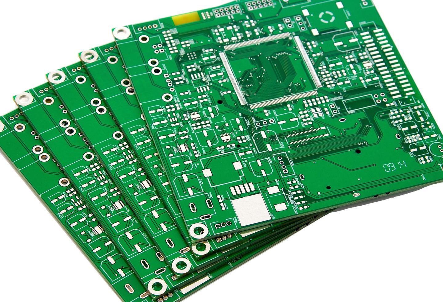
PCB (printed circuit board) is an indispensable component in electronic devices. It not only provides physical support for electronic components, but also realizes the electrical connection between them. From simple household appliances to complex aerospace equipment, PCBs are everywhere, and their manufacturing process involves multiple steps, each of which is crucial and directly related to the performance and quality of the final product.

Design phase
PCB manufacturing begins in the design phase. Professional circuit design engineers use electronic design automation (EDA) software such as Altium Designer, Cadence Allegro, etc. to convert circuit schematics into PCB layouts. During the design process, engineers need to comprehensively consider factors such as the size, shape, number of layers, and layout of components of the circuit board to ensure that the circuit board achieves the best electrical performance, heat dissipation, and mechanical strength. At the same time, relevant design specifications and standards, such as IPC (International Electronic Industry Connection Association) standards, must be followed to ensure the reliability and manufacturability of the design.
Material preparation
After the design is completed, the next step is to prepare the materials needed to manufacture the PCB. The most basic material is the core board, which is usually made of copper-clad laminate. Its material is mostly FR-4 (epoxy glass fiber board), which has good insulation, heat resistance and mechanical strength. In addition, it is necessary to prepare a semi-cured sheet (Prepreg) for multilayer board manufacturing. It is an uncured epoxy resin sheet used for interlayer bonding. For PCBs with special requirements, such as high-frequency circuit boards, special high-frequency materials such as Rogers are also required.
Manufacturing stage
▶Copper cladding
Copper cladding is the first step in PCB manufacturing. It is achieved by covering the surface of the core board with a thin layer of copper foil. For double-sided copper-clad boards, copper foil is required on both the upper and lower surfaces of the core board. There are two main ways to clad copper: electroplating and chemical deposition. Electroplating copper cladding is to use the core board as the cathode and place it in a copper salt solution. Under the action of an electric field, copper ions are deposited on the surface of the core board to form a copper layer. Chemical deposition copper cladding is to generate a copper layer on the surface of the core board through a chemical reaction without the need for an electric field. The thickness of the copper clad is generally between 18 microns and 70 microns, and the specific thickness is determined according to the design requirements.
▶Etching
Etching is a key step in forming a circuit pattern. First, a layer of photosensitive film is covered on the surface of the copper clad board, and then the designed circuit pattern is transferred to the photosensitive film by photolithography. Next, the copper clad board is placed in an etching solution. Under the protection of the photolithography pattern, the unprotected copper layer will be corroded by the etching solution, thereby forming the required circuit conductors, pads, and vias. Commonly used etching solutions include ferric chloride and copper sulfate. During the etching process, the concentration, temperature, and etching time of the etching solution must be strictly controlled to ensure the accuracy and quality of the circuit pattern.
▶Drilling
The purpose of drilling is to form vias on the PCB to achieve electrical connections between multilayer boards. According to the design requirements, a professional drilling machine is used to drill the required holes on the PCB. The diameter of the drill hole is generally between 0.1 mm and 3 mm, and the accuracy requirement is relatively high. During the drilling process, attention should be paid to the selection of the drill bit, the control of the drilling speed, and the use of coolant to avoid problems such as drill bit damage and PCB overheating.
▶Electroplating
Electroplating is mainly used to form a uniform metal layer on the inner wall of the via and the surface of the circuit pattern to enhance the reliability of the electrical connection and the solderability of the pad. Common electroplated metals include copper, nickel, gold, etc. The electroplating process needs to be carried out in a specific electroplating solution. The thickness and quality of the electroplating layer are controlled by adjusting the composition, temperature, current density and other parameters of the electroplating solution. The thickness of the electroplating layer is generally between 1 micron and 30 microns, and the specific thickness is determined according to the application requirements.
▶Solder mask
The purpose of solder mask is to form a protective film on the surface of the PCB to prevent solder from adhering to places where soldering is not required during welding, and to protect the circuit from the influence of the external environment. The solder mask is usually made of photosensitive solder mask ink. First, a layer of solder mask ink is evenly coated on the surface of the PCB, and then the designed solder mask pattern is transferred to the solder mask ink by photolithography. After exposure, development and other processes, the unexposed solder mask ink will be washed away to form the desired solder mask pattern. The thickness of the solder mask is generally between 20 microns and 50 microns. It is necessary to ensure good adhesion to the PCB surface and no defects such as bubbles and particles.
▶Silkscreen
Silkscreen is the process of printing information such as component identification, pad identification, and circuit identification on the surface of the PCB. Through screen printing, special ink is transferred to the surface of the PCB through the screen. The precision of silkscreen printing is high, and the characters must be clear and the position must be accurate. Silkscreen ink generally has good wear resistance and corrosion resistance to ensure that the identification information is not worn or corroded during the use of the PCB.
▶Cutting
Cutting is the process of separating the manufactured PCB from the entire board. According to the shape and size requirements of the PCB, professional cutting equipment such as V-cut, milling cutter, etc. are used to cut the PCB into the required shape. During the cutting process, attention should be paid to cutting accuracy and cutting quality to avoid damage to the PCB. At the same time, the flatness and smoothness of the edge of the PCB after cutting should also be considered to meet the requirements of subsequent assembly and use.
Testing phase
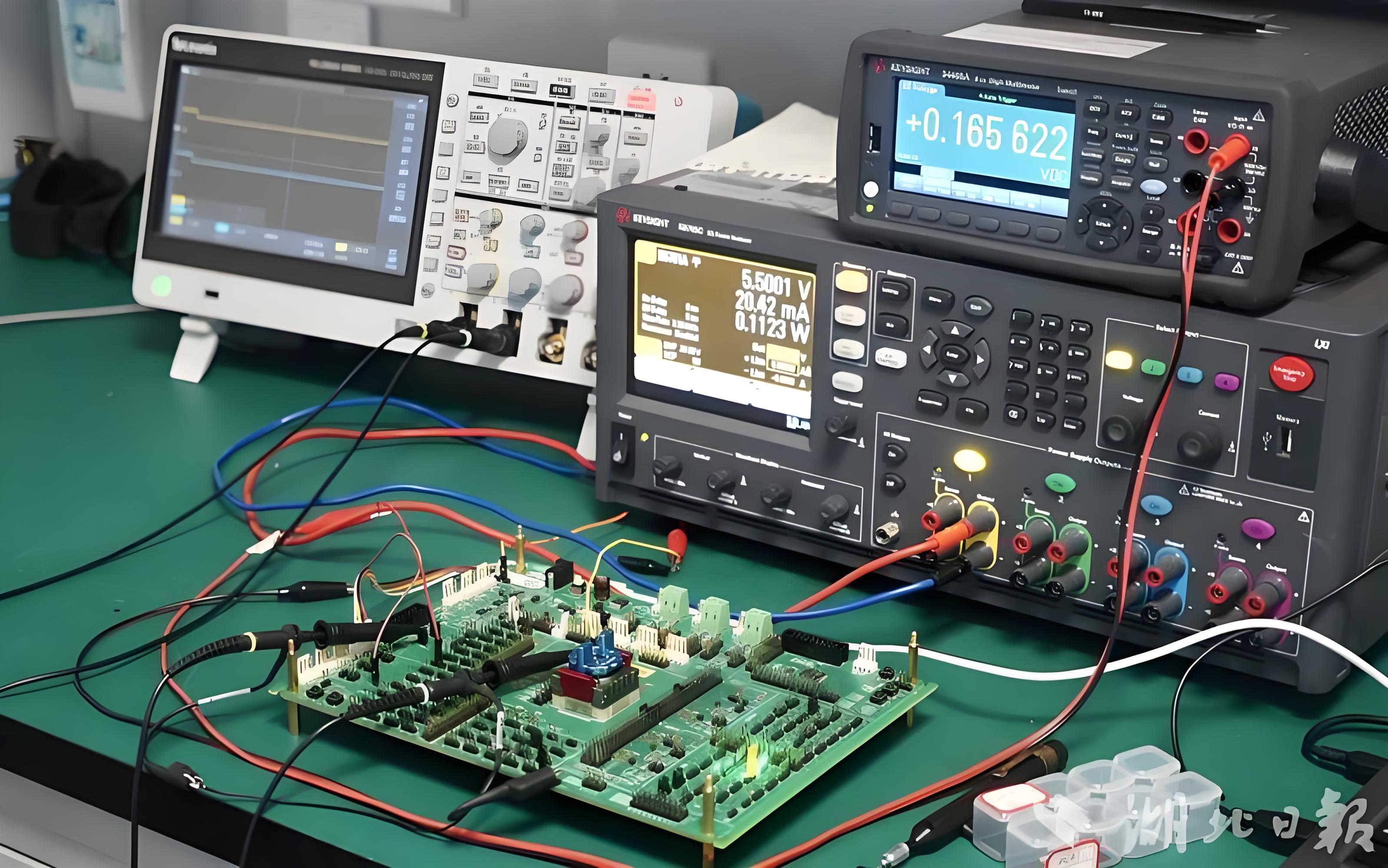
After the PCB is manufactured, it needs to be rigorously tested to ensure that its performance and quality meet the design requirements. Common test items include electrical testing, functional testing, environmental testing, etc. Electrical testing mainly detects whether the electrical parameters of the PCB, such as conductivity, insulation, impedance, etc., meet the standards. Functional testing simulates the operation of the PCB in the actual working environment to detect whether it can work normally. Environmental testing includes high temperature testing, low temperature testing, wet heat testing, etc., which are used to evaluate the stability and reliability of the PCB under different environmental conditions. Through these tests, problems in the PCB manufacturing process can be discovered in time, and corresponding improvements and repairs can be made, thereby improving the overall quality and reliability of the product.

